SINCHON·INT′l
SINCHON·INT′l
- MIRAE

show mobile menu
mobile menu
Commercializing Next-Generation 2D Semiconductors in Practice
The research team led by Professor Seongil Im developed a 2D super-thin nano CMOS device.
The research team led by Professor Seongil Im at the Department of Physics, Yonsei University, successfully converted the conductivity type of a transistor device on a selective manner based on a single 2D semiconductor piece, using a stable hydrogen doping method so called atomic layer deposition. This indicates that the potentials for commercialization of 2D semiconductor devices have significantly improved.
Monolayer molybdenum ditelluride (MoTe2) is a transition metal dichalcogenide composite, one of the most well-known 2D semiconductor materials. Since MoTe2 has an interlayer bonding with a van der Waals force just like graphene, which won the Nobel Physics prize in 2010, it can be formed as 2D by mechanical detachment. Unlike graphene, which has nearly no bandgap and thus is difficult to be used as a semiconductor material, MoTe2 has a bandgap close to that of silicon. That is why there has been increasing research on the material as an alternative to silicon. However, it still has a shortcoming; a stable production of N- and P-type semiconductors is challenging, which makes it difficult to be directly commercialized.
The research team observed that the characteristics of a p-type device were converted to those of an n-type device, after a hydrogen doping treatment on a nanometer-scale MoTe2 channel using the atomic layer deposit technique. In particular, the converted n-type semiconductor showed an increased current as well as stability of the transistor device depending on the hydrogen doping.
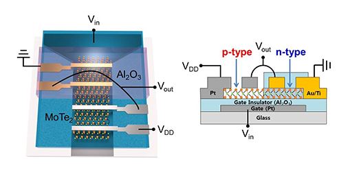
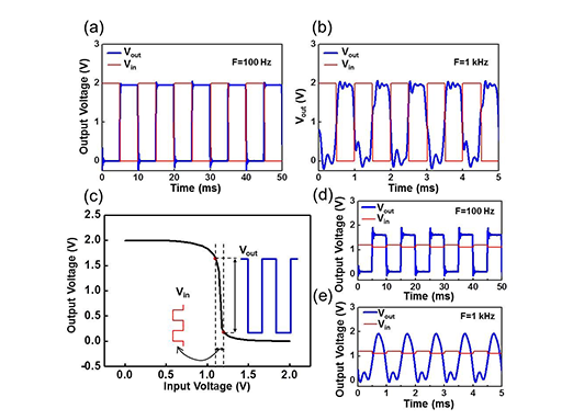
The detailed mechanism of hydrogen doping, that is, how hydrogen doping creates n-type carriers, is identified by detailed calculation of a research team led by Professor Hyoung Joon Choi at Yonsei University. By performing selective hydrogen doping on the necessary places based on these results, the team created stable n-type and p-type devices at the same time, through which a CMOS (complementary metal–oxide–semiconductor) inverter, the most basic logic circuit, was successfully constructed. The circuit was confirmed to be functioning stably both at DC and AC voltages.
Professor Im said, “since the hydrogen doping discovered in this research uses a stepper exposure process and atomic layer deposit technique, which both are commonly used in the conventional silicon semiconductor industry, the results of this research can be especially significant in commercialization of next-generation 2D semiconductors in practice.”
This research was supported by the Projects to Encourage Leading Researchers and the Projects for Leading Science Research Centers sponsored by the Ministry of Science, ICT and Future.
Recommended Articles

Professor Byeong-Su Kim
New study demonstrates that “deformable” electronics are not a stretch

Professor Yeonjin Yi


