SINCHON·INT′l
SINCHON·INT′l
- MIRAE

show mobile menu
mobile menu
A van der Waals Heterostructure Device Platform Opens a New Chapter for 2D Semiconductors
A joint research team led by Professor Gwan-Hyoung Lee successfully observed quantum transport in a 2D semiconductor for the first time in the world.
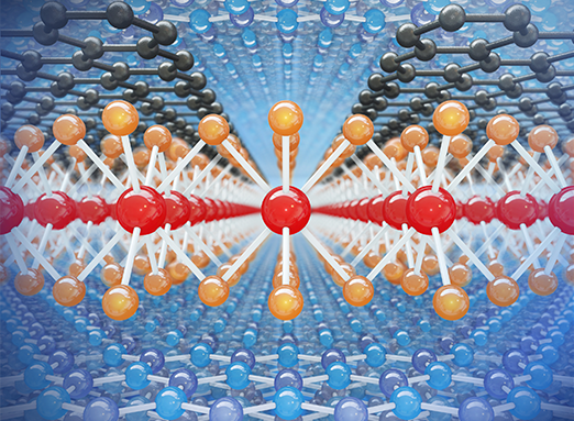
A joint research team of Yonsei University and Columbia University successfully observed the movement of electric charges and quantum transport in the thinnest semiconductor in the world using a novel van der Waals heterostructure device platform. Professor Gwan-Hyoung Lee, who has been leading this research, developed the new device structure that has a thin and smooth interface with a thickness of a few atomic layers, by stacking molybdenum disulfide (MoS2, a future-generation semiconductor material that is gaining increasing attention), graphene (electrical contacts), and hexagonal boron nitride (hBN, dielectric). Through this development, he proved the possibility of creating a high-performance, low-power-consumption, and high-speed quantum device of super-thin semiconductors. This research is expected to contribute to strengthening the competitiveness of the semiconductor and information and communication technology (ICT) industries.
Since two scientists at Manchester University won a Nobel Prize for their discovery of graphene in 2010, there have been active efforts globally to study 2D semiconductor materials. Against this backdrop, more studies have been made in recent days that show the possible applications of 2D semiconductor materials in various devices. However, the characteristics of the devices have often failed to fulfill their theoretical performance. Recognizing this problem, Professor Lee began the research by developing a standard material structure that can evaluate the intrinsic nature of 2D semiconductor materials in order to assess their performance limit, and to ultimately develop new devices.
“As the silicon-based semiconductor industry keeps growing, there have been increasing calls for flexible and transparent devices. That is how graphene was developed, followed by active research efforts in relevant fields. But graphene has a shortcoming; it does not have a bandgap. For the continuous growth of the semiconductor industry, there should be a graphene-like material with a bandgap. Such a material is MoS2, reported in 2011. I focused on these 2D semiconductor materials as I began this research, because I thought new devices could be developed by utilizing unique characteristics of these materials and applying a multi-layered structure.”
This study developed a standard device structure that dramatically enhances the charge carrier mobility in the thinnest semiconductor in the world. This study is significant compared to existing studies in that it lays foundations for the development of high-performance electronic devices and innovative quantum devices. Professor Lee conducted a joint project with Professor James Hone’s team at Columbia University and Professor Chul-ho Lee at Korea University, and developed a new device structure with a thin, smooth interface using the multi-layered van der Waals heterostructure. They observed the highest carrier mobility that have ever been measured and succeeded in observing quantum transport in a 2D semiconductor for the first time in the world.
The research, which was conducted jointly with a Columbia team led by Professor James Hone and Professor Chul-ho Lee at Korea University, was published on the online issue of Nature Nanotechnology, a world-renowned academic paper in the field of nanoscience, on April 27th 2015.
Recommended Articles
Professor Jong-Hyun Ahn
Novel technique for producing high-resolution micro-LED displays

Professor Seong Chan Jun

Professor Donghyun Kim
Array of hope: Up close and personal with mitochondria in neurons


